
SemiconducThe semiconductor fabrication processes are the foundation of today’s technological advancements. Every smartphone, laptop, and satellite relies on semiconductors for their functionality. This highly complex and precise process transforms raw silicon into the microchips that enable our digital world. By understanding the steps involved, the challenges faced, and future innovations, we can appreciate the incredible science behind the devices we use daily.
What is Semiconductor Fabrication?
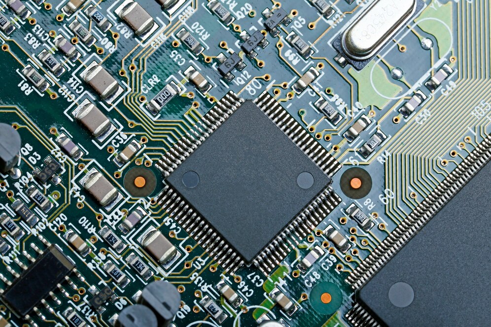
Semiconductor fabrication refers to the precise creation of integrated circuits (ICs) on a silicon wafer. This meticulous process involves multiple steps, such as material addition, removal, and modification, to construct the essential components that make up a functional chip.
Key Steps in the Semiconductor Fabrication Process
1. Wafer Preparation
The journey begins with the preparation of pure silicon wafers.
- Purification: Silicon is refined to an ultra-high-purity level to ensure flawless performance.
- Slicing: Cylindrical silicon ingots are carefully sliced into thin, flat wafers.
- Polishing: The wafers are polished to a mirror-like finish for precise manufacturing.
2. Oxidation
A silicon dioxide layer is formed on the wafer’s surface to provide electrical insulation. This step is critical for creating controlled regions within the chip.
3. Photolithography
This step defines the intricate patterns of the chip.
- Coating: A photosensitive material, called photoresist, is applied to the wafer.
- Exposure: UV light passes through a photomask, imprinting the desired pattern.
- Development: Exposed photoresist is removed, revealing the chip’s structural design.
4. Etching
Etching removes unwanted materials from the wafer to refine the circuit design.
- Wet Etching: Liquid chemicals dissolve specific layers.
- Dry Etching: Plasma is used for high-precision material removal.
5. Deposition
Adding material layers is vital for constructing the chip.
- Chemical Vapor Deposition (CVD): Creates thin, uniform layers of material.
- Physical Vapor Deposition (PVD): Deposits metals for electrical pathways.
6. Ion Implantation
This process introduces ions into specific areas to adjust electrical properties, enabling the creation of semiconductor junctions.
7. Metallization
Metallic layers connect the chip’s components, ensuring proper electrical functionality. Aluminum and copper are common materials used.
8. Packaging and Testing
- Dicing: The wafer is cut into individual chips.
- Encasing: Each chip is packaged for protection and connectivity.
- Testing: Rigorous testing identifies defective chips and ensures performance reliability.
Advanced Techniques in Semiconductor Fabrication
Extreme Ultraviolet (EUV) Lithography
EUV lithography allows for smaller, more precise designs by utilizing shorter wavelengths of light.
3D Stacking and TSVs
Three-dimensional stacking increases performance by layering multiple chips vertically, reducing space and enhancing speed.
Sub-10 Nanometer Processes
Modern fabrication at sub-10 nm scales allows for higher transistor density, better performance, and reduced power consumption.
Challenges in Semiconductor Fabrication
Despite its remarkable capabilities, semiconductor fabrication has its share of challenges:
- Astronomical Costs: Setting up and maintaining fabrication facilities can cost billions of dollars.
- Precision Demands: Manufacturing at nanometer scales requires an almost zero-error approach.
- Material Constraints: With silicon nearing its physical limits, new materials like graphene are being explored.
- Heat Dissipation: High transistor densities generate significant heat, necessitating advanced cooling techniques.
The Future of Semiconductor Fabrication
Quantum Computing Chips
Quantum semiconductors promise to revolutionize computing by leveraging qubits for tasks beyond the scope of traditional chips.
Sustainability and Efficiency
Manufacturers are exploring greener production techniques to reduce waste and energy consumption.
AI-Driven Fabrication
Artificial intelligence is streamlining chip design and optimizing manufacturing processes, resulting in faster and more efficient production.
FAQs
It’s the process of creating integrated circuits using a series of precise steps on silicon wafers.
Photolithography defines the circuit patterns on a chip, allowing for precise and intricate designs.
Key challenges include high costs, precision demands, heat dissipation, and the physical limits of silicon.
Techniques like EUV lithography, 3D stacking, and sub-10 nm processes enable the production of cutting-edge chips.
AI optimizes chip design, predicts errors, and automates parts of the manufacturing process, improving efficiency.
Conclusion
Semiconductor fabrication processes combine science, engineering, and innovation to power the digital age. From smartphones to AI systems, these microchips are integral to modern life. As the industry evolves, advancements like quantum computing, greener manufacturing, and AI-driven techniques promise to shape the future of this transformative field.
For further exploration, check out our resources on VLSI technology.
Suggestions
- Learn about EUV Lithography at ASML.
- Stay updated on quantum semiconductor trends via IEEE Spectrum.
